Component Pinouts and Notes
- 78L05 Voltage Regulator in TO-92 package
- LM358 and TL072 Dual Op Amps
- TL074 Quad Op Amp
- MAX495 Op Amp
- Arduino Nano
- IRF3205 MOSFET in TO-220 package
This page will list pinouts of some electronic components I commonly find myself using, as well as some notes on using them that might not be obvious from reading the datasheets.
78L05 Voltage Regulator in TO-92 package
Datasheet (pdf) for L78L series voltage regulators which includes the 78L05
The 78L05 provides a regulated 5v supply on its output pin if sufficient voltage (at least 7v) is supplied to its input. If a device’s documentation says that the device requires a regulated 5v power supply, this is the kind of thing that it means.
The TO-92 package is commonly used for transistors but other 3-pin components can also be found in this package.
The pinout in the datasheet is from the bottom-up point of view which I found counterintuitive and possibly dangerous for people skimming the manual looking for a pinout without reading the text indicating it’s a bottom-up view. In my experience, when a voltage source is connected to the output pin of 78L05 (ie. when it is connected backwards), the same voltage can be measured at its input pin. It’s not clear how much current it will allow to flow when connected backwards but it’s possible that this could damage whatever component is being powered by the incorrectly connected 78L05.
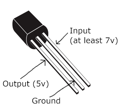
The component has a round side and a flat side. As shown in the image above, with the flat side facing you, with the pins pointing downwards:
- The left pin is the output and will provide 5v if sufficient voltage (at least 7v) is supplied to the input.
- The middle pin is ground.
- The right pin is the input.
The figure of 7v as the minimum input voltage is based on this image from the manual:
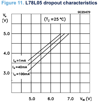
So the actual minimum input voltage depends on how much current is being drawn from the output, but if it’s up to 100mA then 7v will be fine.
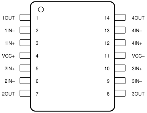
LM358 and TL072 Dual Op Amps
Datasheet (pdf) for LM385 Dual Op Amp (also contains information on related components)
Datasheet (pdf) for TL072 Dual Op Amp (also contains information on related components)
Both components include a pair of op amps on a single chip and they have identical pinouts. This is the pinout viewed from top-down:
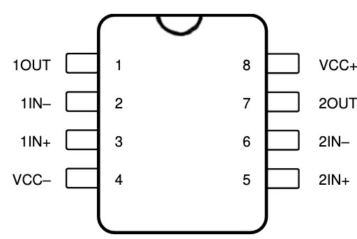
This table lists the pins corresponding to their arrangement in the diagram above. The semi-circular indentation on the top of the IC is facing upwards.
| Left Side | Right Side |
|---|---|
| 1OUT | VCC+ |
| 1IN- | 2OUT |
| 1IN+ | 2IN- |
| VCC- | 2IN+ |
My mnemonic for this pinout is that the bottom left is usually ground and the top right is usually positive voltage for ICs, and if you don’t have a negative supply voltage you’ll probably connect the VCC- pin to ground. Then, a common op amp feedback configuration is a voltage forwarder (aka. a buffer amplifier) and in this configuration the IN- pin and the OUT pin are connected together. I like to pretend that the designer wanted to make it easy to setup a voltage forwarder by putting the OUT and IN- pins next to each other for both op amps on the chip.
TL074 Quad Op Amp
Datasheet (pdf) for TL074 Quad Op Amp (also contains information on related components)
This is 4 op-amps in a single chip. This is the pinout viewed top-down:
This table lists the pins corresponding to their arrangement in the diagram above. The semi-circular indentation on the top of the IC is facing upwards.
| Left Side | Right Side |
|---|---|
| 1OUT | 4OUT |
| 1IN- | 4IN- |
| 1IN+ | 4IN+ |
| VCC+ | VCC- |
| 2IN+ | 3IN+ |
| 2IN- | 3IN- |
| 2OUT | 3OUT |
MAX495 Op Amp
Datasheet (pdf) for MAX495 Op Amp (also contains information on related components)
This Op Amp is marketed as “Rail to Rail” which means its min and max outputs are close to the + and - supply voltages.
In the pinouts below I’ve added VCC- and VCC+ labels in addition to the VEE and VCC labels from the manual for consistency with other component pinouts.
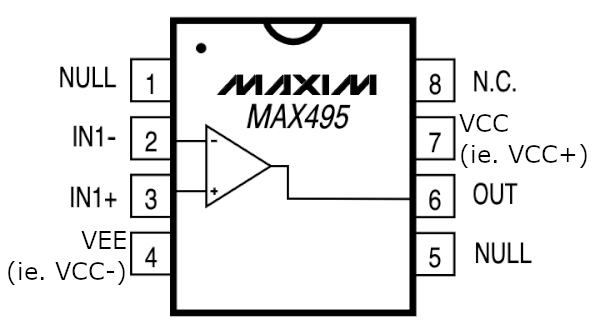
This table lists the pins corresponding to their arrangement in the diagram above. The semi-circular indentation on the top of the IC is facing upwards.
| Left Side | Right Side |
|---|---|
| NULL | N.C. |
| IN1- | VCC (ie. VCC+) |
| IN1+ | OUT |
| VEE (ie. VCC-) | NULL |
The inputs are numbered even though there is only one op-amp on the chip. The output is not numbered in the manual but it could just as well be called OUT1.
The NULL pins are not the same as the N.C. (Not Connected) pin. The NULL pins can be used to adjust something called “input offset voltage”. There’s more info in the manual.
Arduino Nano
Datasheet (pdf) for Atmel Atmega328P (the microcontroller on the Arduino Nano
Arduino Nano Pinout
This is the pinout of the Arduino Nano from the Arduino documentation, except I’ve modified it to clarify that pins A6 and A7 can’t be used as digital I/O port pins.
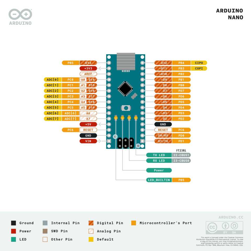
Here’s the pinout in tabular form. The positions of pins correspond to a top-down view of the Arduino Nano with the usb port facing upwards. Each entry is named after what is literally printed on the PCB next to each pin. In parentheses after each name are the I/O port pin function (PXn) and the ADC channel (ADCn) if any.
| Left Side | Right Side |
|---|---|
| D13 (PB5) | D12 (PB4) |
| 3V3 | D11 (PB3) |
| REF | D10 (PB2) |
| A0 (PC0, ADC0) | D9 (PB1) |
| A1 (PC1, ADC1) | D8 (PB0) |
| A2 (PC2, ADC2) | D7 (PD7) |
| A3 (PC3, ADC3) | D6 (PD6) |
| A4 (PC4, ADC4) | D5 (PD5) |
| A5 (PC5, ADC5) | D4 (PD4) |
| A6 (ADC6) | D3 (PD3) |
| A7 (ADC7) | D2 (PD2) |
| 5V | GND |
| RST (PC6) | RST (PC6) |
| GND | RX0 (PD0) |
| VIN | TX1 (PD1) |
Arduino Nano Power Supply
You can power the Arduino Nano by supplying between 7 and 12 volts to the VIN pin, or by supplying regulated 5 volts to the 5V pin (such as with a 78L05 voltage regulator). When powering via the VIN pin, the 5V pin can be used as a 5V power supply for powering other components (including other Arduino Nanos, in which case you would connect the 5V pin on one Arduino Nano to the 5V pin on other other). This works because in between the VIN and 5V pins there is a 5v voltage regulator similar to the 78L05 (but not identical - the Arduino Nano uses a LM117IMPX-5.0). It supplies the Arduino with regulated 5V but can supply other things too via the 5V pin, because its output connects directly to this pin.
Some sources will recommend against supplying your own voltage regulator and powering via the 5V pin and using the VIN pin instead. Indeed there is little point using the 5V pin as the onboard voltage regulator should be just as good as whatever you use instead to produce the regulated 5v. One reason you might do this anyway is because the voltage regulator could wear out over time and it’s much cheaper to replace a voltage regulator than an entire Arduino. You could wait until the onboard regulator fails before circumventing it with an external component but this might be hard once the Arduino is soldered in place compared to replacing the external voltage regulator with a new one.
Arduino Digital Pins
The Arduino Digital Pin documentation is a good starting point.
Some of the pins are multiplexed and have other functions that prevent them from operating as digital IO pins, but by default all digital pins behave as IO pins.
There are 3 registers per IO port with a bit for each pin:
DDx(Data Direction) determines whether a pin is an input pin or an output pin. 0 = input, 1 = output. The default is all 0s (all input pins).PINxcan be read to determine the state of input pins.PORTxcan be written to set the state of output pins. Writing a 1 to a bit in this register corresponding to an input pin enables the pull-up resistor for that pin.
Arduino Switch Configurations
The main consideration when attaching buttons is not letting the input pin “float”; the pin should always be connected to a voltage source or ground. This is the purpose of “pull-up” and “pull-down” resistors. The resistor connects the pin to the voltage source that will represent the “off” state (this could be logic 1 or logic 0), and then when the button is pressed, the pin is connected directly to the voltage source representing “on”.
Here is an example where the input pin sees 0v via the 10K pull-down resistor to ground, but when the button is pressed the pin sees 5v.
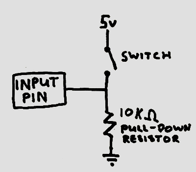
Note that input pins have very high impedance, so they draw almost no current. We don’t have to worry about connecting a voltage source directly to the pin.
Here’s another example where the input pin sees 5v via the 10K pull-up resistor, but when the button is pressed the input pin sees 0v.
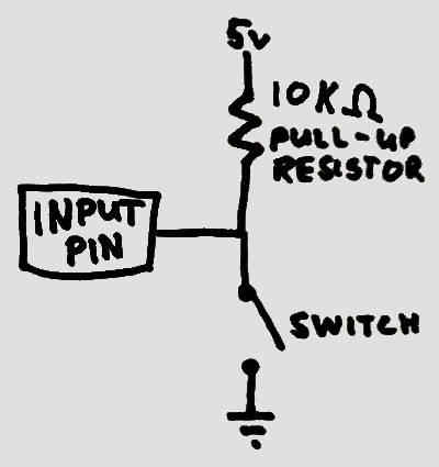
When the switch is open the pin sees (almost) the full 5 volts because the pin has incredibly high impedance; it basically acts like an open circuit for the purposes of calculating current and voltage drop.
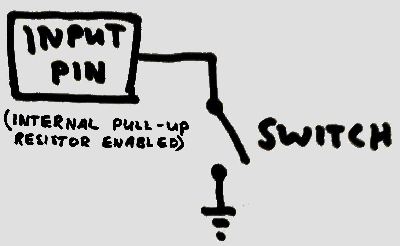
This example shows how one could connect a switch with the Arduino’s internal pull-up resistor enabled (write a 1 to the PORTx bit for the input pin). The following example is functionally equivalent to the previous example, but the pull-up resistor is inside the Atmega328P chip on the Arduino.
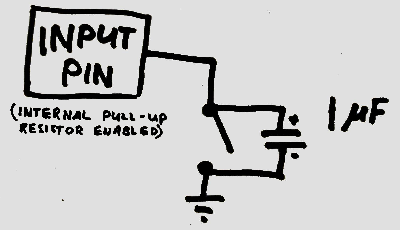
When dealing with physical switches, one problem that can happen is “bouncing” which is when the physical connection rapidly closes and opens for a brief period after the switch is pressed. This can be solved in software by introducing a short delay where the switch is ignored for a brief period after its state changes, or it can be solved in hardware by adding a capacitor in parallel with the switch. The charging and discharging of the capacitor smooths out the rapid connecting and disconnecting, and the pin only sees the state change after enough time has passed for the capacitor to charge or discharge (depending on whether a pull-down or pull-up resistor is being used).
This example shows how to connect a capacitor to the internal pull-up resistor example above, though the same technique can be used for all the examples.
Mixing Output Pin Values
This demonstrates a way of mixing the voltages at two output pins by connecting them together through resistors to a common node. The diagram below shows two pins connected in this way but it works for arbitrarily many pins. If the resistors all have the same resistance then the common node will have a voltage that is the mean of voltages at the output pins, but using different resistors results in the weighted mean instead.
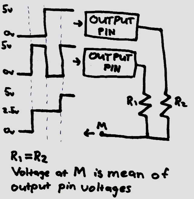
This works because unlike input pins which have very high impedance, output pins have very low impedance (both when acting as current sources and current sinks). This means that they can produce relatively large amounts of current (the docs say 40mA) and also they can consume a lot of current. This means that when an output pin is producing logic 0 (0v), it serves a similar role to ground (it has 0v and it’s a current sink). Thus we can analyse the circuit above as we would a simple voltage divider. When one output is low and one output is high, then half the high voltage is seen between the two resistors provided that they have the same resistance.
This idea can be extended to implement a digital to analog converter by combining the voltages of many pins through carefully chosen resistances.
Note that as with naive voltage divider circuits (this is really just a naive voltage divider circuit) the output of this circuit (the node with mixed voltage) has high impedance (due to the resistors used). This means its voltage will rapidly reduce as current is drawn through that node of the circuit. One way to fix this problem is to connect it to a voltage forwarder op-amp configuration:
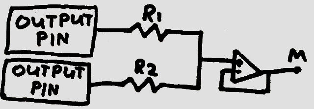
Note that at this point we have almost implemented a non-inverting voltage adder (a common op-amp configuration). All that’s missing are resistors in the feedback network to increase the gain of the op-amp to be equal to the number of pins being combined. With a voltage forwarder the gain is 1 so its output is the (possibly weighted) mean of voltages rather than the (possibly weighted) sum of voltages.
Arduino Analog Pins
The ADC can be configured to use an internal reference voltage by setting the
REFS0 and REFS1 bits of the ADMUX register, avoiding the need to connect
a reference voltage to the AREF pin. To use the supply voltage as the
reference voltage, use the “AV CC with external capacitor at AREF pin” by
setting REFS0 and REFS1 to 1 and 0 respectively. In this configuration,
connect a 100nF capacitor between AREF and ground to reduce noise.
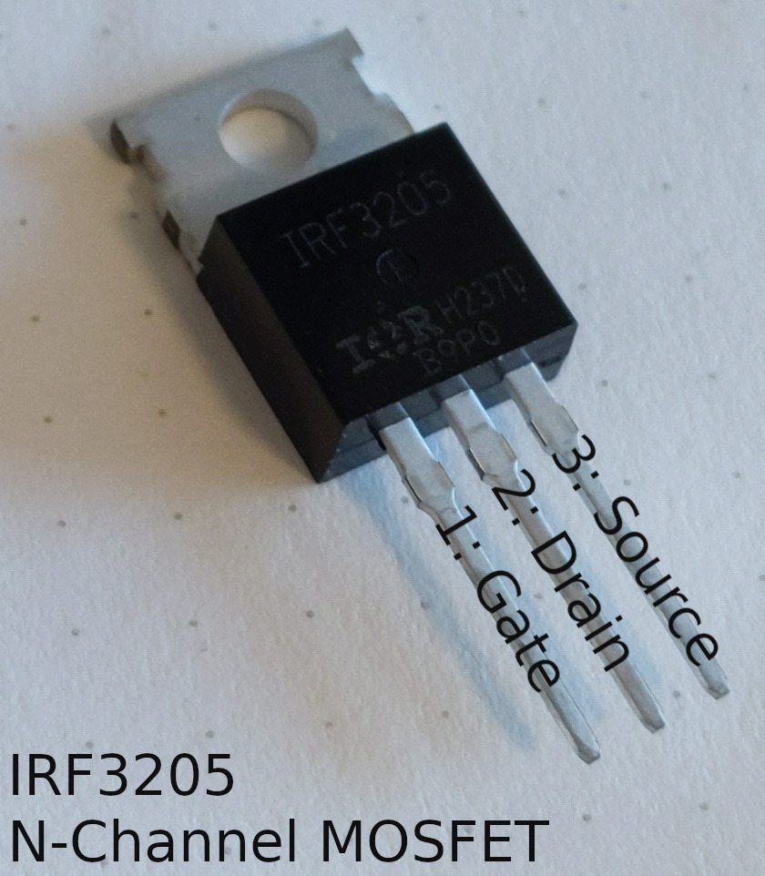
IRF3205 MOSFET in TO-220 package
The IRF3205 is an N-Channel MOSFET.
Facing the front of the component (ie. the text is visible) with the pins pointing downwards, the pinout from left to right is:
- Gate
- Drain
- Source